
Global Commercial & Industrial Status of Semiconductor Heating Strips
Thermal processing lies at the heart of semiconductor fabrication. As sub-5nm lithography nodes and multi-layer 3D NAND architecture drive microelectronics manufacturing, the demand for high-purity, long-life semiconductor heating strips engineered from advanced resistance alloys has expanded exponentially worldwide.
Sub-Nanometer Thermal Precision
Modern semiconductor fabrication equipment—including Chemical Vapor Deposition (CVD), Atomic Layer Deposition (ALD), MOCVD, and Oxidation/Diffusion vertical furnaces—requires thermal uniformity within ±0.1°C across 300mm silicon wafers. High-precision resistance strips serve as the primary heating elements to prevent thermal stress, crystal dislocations, and film thickness variance.
Ultra-Cleanroom & Low Outgassing
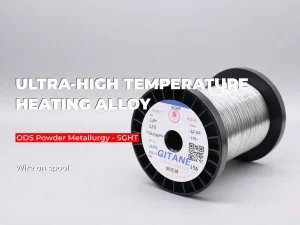
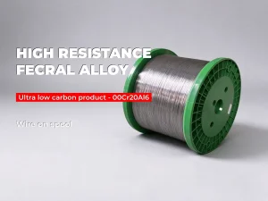
Traditional heating elements release microscopic metal particles, volatile carbon contaminants, or heavy element outgassing at high temperatures. Semiconductor heating strips produced from ultra-low carbon FeCrAl (such as 00Cr20Al6) and powder-metallurgy SGHT alloys generate a dense, self-healing α-Al2O3 protective oxide layer, eliminating particulate contamination inside ISO Class 1 cleanrooms.
Geopolitical Supply Chain Resilience
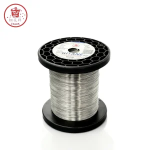
With global semiconductor supply chains restructuring, equipment original equipment manufacturers (OEMs) in North America, Europe, and Asia are sourcing certified Chinese manufacturers. Beijing Shougang Gitane New Materials Co., Ltd. (SPARK) delivers ISO 9001 and GB/T 1234-2012 certified resistance heating ribbons, offering an optimal balance of structural strength, oxidation endurance, and cost efficiency.
Where Semiconductor Heating Strips Drive Yields
From silicon crystal growth to micro-chip packaging, specialized electrical resistance heating strips fulfill crucial thermal profiles across every step of wafer manufacturing.
1. Vertical Diffusion & Thermal Oxidation Furnaces
In high-temperature wafer oxidation, annealing, and drive-in diffusion, vertical furnaces utilize coiled or meander-patterned FeCrAl heating strips (0Cr25Al5, HRE, or SGHT). Operating continuously between 900°C and 1350°C, these flat strips maximize heat radiation surface area compared to round wire, ensuring extreme radial temperature uniformity across dozens of stacked 300mm wafers simultaneously.
2. MOCVD & SiC/GaN Epitaxial Growth Reactors
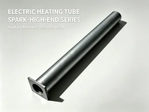
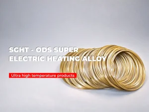
Wide-bandgap semiconductors (Silicon Carbide and Gallium Nitride) require extreme temperatures exceeding 1200°C–1400°C for single-crystal epitaxial layer growth. Powder metallurgy SGHT grade FeCrAl heating ribbons and tubes handle intense hot-gas environments and aggressive hydrogen thermal cycling without sagging, structural creep, or grain boundary degradation.
3. ALD/CVD Pre-Heat & Gas Line Thermal Tracing
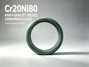
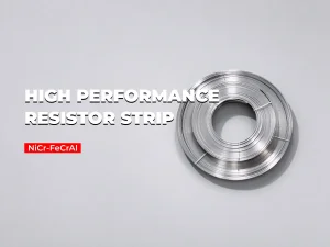
Atomic Layer Deposition (ALD) relies on precise precursor gas delivery without premature condensation. Flexible NiCr ribbons (Cr20Ni80) and thin-gauge resistance strips are jacketed around stainless steel gas feed lines, vacuum manifolds, and exhaust valves, providing steady, spark-free low-voltage trace heating between 150°C and 450°C.
4. Photolithography Wafer Track Bake Plates
Prior to and following optical exposure, wafers undergo Soft Bake and Post-Exposure Bake (PEB) on precision hot plates. Embedded flat resistance heating ribbons deliver rapid ramp-up rates (>50°C/s) and fast thermal response times, enabling tight Critical Dimension (CD) control in photoresist processing.
Metallurgical Analysis: FeCrAl vs. NiCr Alloys for Semiconductor Equipment
Engineers must carefully evaluate mechanical strength, maximum operating temperature, electrical resistivity, and oxide film dynamics when specifying heating elements for semiconductor capital tools.
| Alloy Grade | Alloy Family | Max Temp (°C) | Resistivity (μΩ·m, 20°C) | Key Oxide Layer | Primary Semiconductor Application |
|---|---|---|---|---|---|
| SGHT Grade | Powder Metallurgy FeCrAl | 1425°C | 1.45 | α-Al2O3 (Adherent Alumina) | High-temp MOCVD, SiC Epitaxy, CVD Chambers |
| SGHYZ / HRE | Rare-Earth FeCrAl | 1350°C - 1400°C | 1.42 | Dense Al2O3 Scale | Vertical Diffusion Furnaces, Sintering |
| 00Cr20Al6 | Ultra-Low Carbon FeCrAl | 1280°C | 1.38 | High-Purity Alumina | Cleanroom Bake Stations, Wafer Track Heaters |
| 0Cr25Al5 | Standard FeCrAl | 1250°C | 1.42 | Al2O3 Oxide Film | General Industrial & Equipment Bakeouts |
| Cr20Ni80 | Nickel-Chromium (NiCr) | 1200°C | 1.09 | Cr2O3 (Chromium Oxide) | Gas Line Tracing, Cycling Hot Plates, Exhaust Lines |
| Cr30Ni70 | High-Cr NiCr Alloy | 1250°C | 1.18 | Cr2O3 Protective Layer | Nitrogen/Inert Atmosphere Chamber Heating |
Why Powder Metallurgy (SGHT)?
Traditional melt ingot alloys suffer from rapid grain growth at temperatures above 1100°C, causing sagging, thermal deformation, and embrittlement. SPARK's SGHT grade utilizes powder metallurgy to embed fine oxide dispersions (Y2O3, ZrO2). This pins grain boundaries, boosting high-temperature creep strength by over 300% and extending heating element operational lifespan under continuous 1400°C load.
Self-Healing Alpha-Alumina Scale
When exposed to ambient or oxygen-rich furnace atmospheres, FeCrAl resistance strips generate a smooth, continuous alpha-alumina (α-Al2O3) scale. This oxide film acts as an electrical insulator and chemical barrier, preventing further atmospheric corrosion and eliminating flaking or spalling that could contaminate sensitive silicon wafers.
Energy Efficiency & Mass Savings
FeCrAl alloys possess a lower density (7.10 g/cm³) compared to NiCr alloys (8.40 g/cm³), combined with a significantly higher electrical resistivity (1.45 vs 1.09 μΩ·m). Equipment designers can utilize thinner heating ribbons to generate equivalent thermal energy, reducing the total thermal mass, shortening ramp-up cycles, and lowering overall fab power consumption.
Global Trends in Semiconductor Thermal Management
As semiconductor manufacturing evolves toward 2nm gate-all-around (GAA) transistors and advanced multi-die packaging, thermal management technology is shifting rapidly.
Trend 1: Zero-Particle Strip Coatings
Next-generation semiconductor tools require electro-polished or surface-passivated resistance ribbons that release zero particulate residue. Advanced pre-oxidation treatment procedures in cleanroom conditions guarantee immediate drop-in compatibility for vacuum chambers.
Trend 2: Multi-Zone Dynamic Heating
To eliminate edge-to-center thermal gradients on 300mm and 450mm wafers, OEMs are migrating from single-loop heaters to 5-zone and 7-zone dynamic heating assemblies using custom-bent meander ribbons engineered to exact resistance tolerances.
Trend 3: Ultra-Fast Rapid Thermal Processing (RTP)
Rapid thermal anneal steps demand thermal ramp rates exceeding 100°C per second. Low thermal mass flat ribbons, combined with high radiant emittance coatings, allow instant thermal turn-on and rapid cool-down without structural warping.
Trend 4: Decarbonized Fab Operations
Semiconductor foundries worldwide are committed to net-zero carbon targets. High-resistivity FeCrAl strips decrease kilowatt-hour energy losses by converting up to 99.8% of electrical input into direct directional radiant heat.
Why Partner with Shougang Gitane (SPARK)
As a core enterprise under the state-owned Shougang Group, Beijing Shougang Gitane New Materials Co., Ltd. brings over six decades of metallurgical innovation, operating an 88,000 m² state-of-the-art manufacturing complex in Beijing, China.
End-to-End Metallurgical Control
From vacuum induction melting (VIM) and electroslag remelting (ESR) to hot rolling, cold precision drawing, bright annealing, and ribbon slitting—every step is completed in-house. This ensures absolute chemical purity, strict grain-size uniformity, and batch-to-batch electrical resistance consistency.
Custom Geometry & Tailored Strips
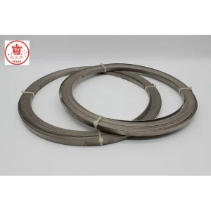
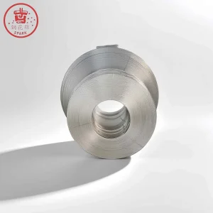
We produce flat heating strips ranging in thickness from 0.05mm to 4.0mm and widths from 0.5mm to 120mm. Tailored surface finishes—including bright annealed, golden oxidized, matte, or cleanroom passivated—are available according to OEM blueprints.
Rigorous QA & International Certification
Certified under ISO 9001:2015, ISO 14001, and ISO 45001, SPARK resistance heating alloys comply strictly with GB/T 1234-2012 standards. Every shipment is accompanied by complete Mill Test Certificates (MTC), detailing spectrographic chemical analysis, tensile strength, and room-temperature electrical resistance.
Frequently Asked Questions (FAQ)
Expert answers to common engineering, procurement, and metallurgical questions regarding China semiconductor heating strips and custom heating element fabrication.
Why are flat resistance heating strips preferred over round wires in semiconductor equipment?
Which alloy grade is recommended for 1300°C+ vertical semiconductor diffusion furnaces?
How does SPARK prevent metallic particle contamination in cleanroom heating applications?
Can SPARK fabricate pre-formed heating element assemblies according to customer drawings?
What is the difference between FeCrAl and NiCr heating strips in nitrogen-containing atmospheres?
What dimensional tolerances and delivery forms are available for wholesale orders?
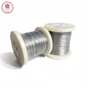
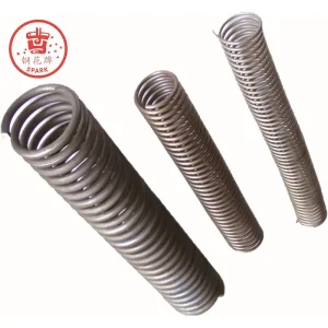
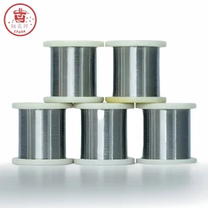
Engineered Heating Strips for Your Next-Gen Semiconductor Tools
Consult directly with Beijing Shougang Gitane’s senior metallurgical engineering team. We provide sample testing, electrical resistance calculations, CAD component prototyping, and factory-direct wholesale quotes.